
https://www.youtube.com/channel/UCRoMhHNzl7tMW8pFsdJGUIA/videos
https://docs.easyeda.com/en/FAQ/Contact-Us/index.html
You are free to use EasyEDA for individuals, business and education.
If you add our Logo and link on your PCB/Video we will appreciate.
Set your project as Private. For extra security you can even save your work locally.
EasyEDA can be run as an offline application.
There are no absolutely secure things in the world but even if you have the misfortune - as happened to one of our team - of losing one laptop and having two hard drives break,
EasyEDA will try to protect your designs in following ways:
We promise to do our best to ensure that neither of these things will happen; we have spent so much of our time to get to this point. We promise that if we cannot make enough money out of EasyEDA to keep it alive or to fund further development, we will not simply abandon our baby or our community but we will consider donating the code to the Open Source Community to let them build on our efforts. There are no companies who can stay forever, so if a time comes when we have to close down, we will follow the steps below:
So, nothing will be lost and our users can continue to enjoy an awesome web based EDA tool that lets them stay in charge of their designs: anywhere, anytime and on any OS.
Please refer at Introduction: Shortcut Keys
Your files are stored on EasyEDA servers, so you can access them anywhere and share them with your partners.
You can download the project via :
EasyEDA is built for people who like to work anywhere, who like to build projects together with other team members, who like to share their projects, who like something that operates like a github for hardware design. The only way to meet these needs is to build a Cloud version EDA.
Although most of the time there are ways to access the internet easily and cheaply there may be times when, for whatever the reason, internet access is simply not possible. For times like this, EasyEDA is working to provide a desktop client soon.
Yes, please refer at: https://easyeda.com/page/download
Chrome and Firefox. If you are restricted to using other browsers, it would be better to download the EasyEDA desktop client.
In the User Center, you can check all your Projects, Modules, Libraries and Friends, Messages etc.
There are two ways to arrive there.


Select it and right click to open a context menu, like the image below.
Select it and right click to open a context menu, like the image below.

1.Make your project public.
Open https://easyeda.com/account/user, move the mouse to the project cover, there is a share icon, click it to share.
2.To share a project privately with only selected collaborators via:
Add Member
The version history of your EasyEDA schematics and PCBs can be accessed by right-clicking on the file you wish to query to open the context menu as shown in the image below:

Then click on the version number that you wish to view.
Note: saving a previous version will restore that version to being the current version of the file.
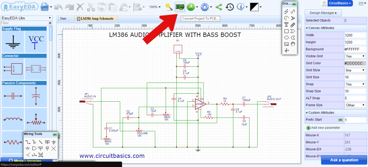
The initial conversion of a schematic to PCB is done from within the Schematic Editor using the Convert Project to PCB... button as illustrated in the toolbar below but a new Update PCB button has been added so that modifications to the schematic can immediately be passed forward to update a selected PCB without having the PCB editor window already open.
Alternatively, you can import changes from the schematic from within the PCB Editor:
https://docs.easyeda.com/en/PCB/Import-Changes/index.html
In this menu, there is a Modify option, so you can rename your files. Double click or right-click the sheet tab can change the sheet title too.
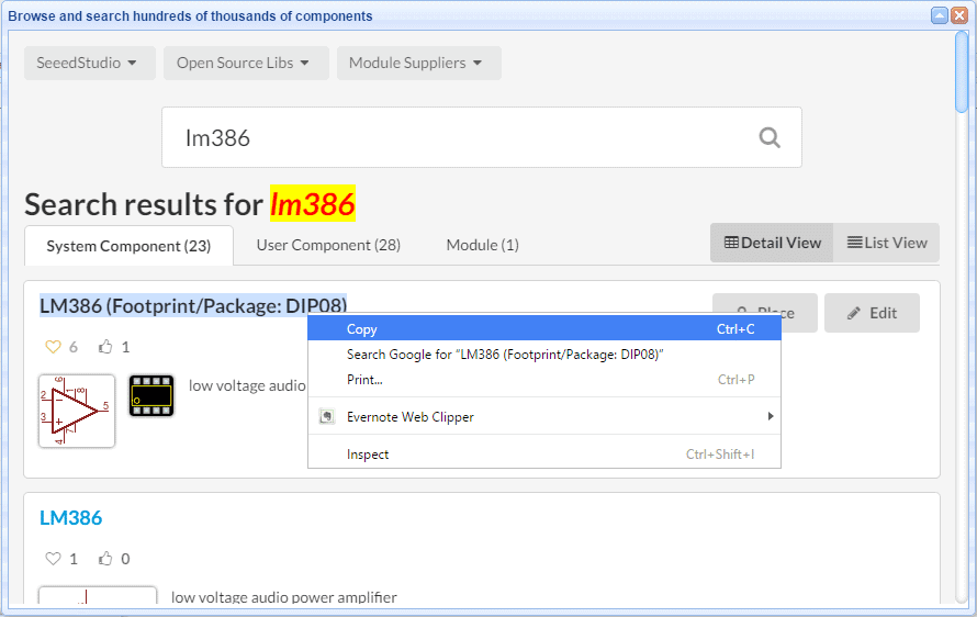
The component search function has been significantly improved to make finding part symbols and footprints quicker and easier. Press SHIFT+F or click on the Libraries icon on the left navigation panel:

In the new components dialog, it is easy to select the right components via tags and you can set tags for your own components.
You can add sub parts to a schematic one by one but please note that the sub parts prefix must be in the form of U1.1 U1.2 etc, and not U1.A U1.B.

The basic unit of the schematic sheet is the pixel. 1 pixel is about 10mil (0.001 inch) but please note that this use of the pixels as a unit in a schematic is just for reference.
EasyEDA don't support hierarchy, but support multi-sheets。
Please check out this link https://docs.easyeda.com/en/Schematic/Multi-Sheet/index.html
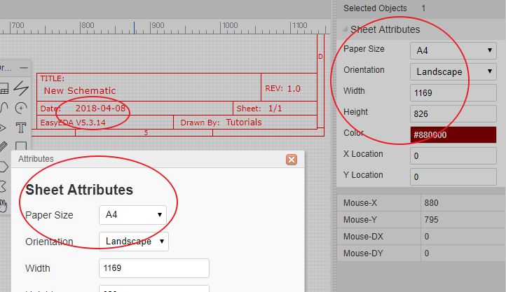
To change the sheet size, move the mouse anywhere over the lower right area of the drawing border or frame until the whole border highlights red and then right-click on it. Paper size and orientation can then be changed in Sheet Attributes in the right hand panel.
To modify the design information, left-click on the relevant blue text in the lower right area of the drawing border or frame to change it in Text Attributes in the right hand panel. Double left-clicking the blue text will allow you to type new information directly into the field.

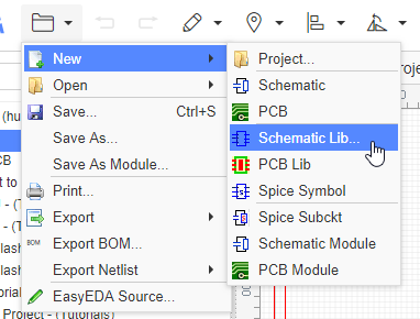
Document > New > Schematic Lib
After creating the library and saving, you can add a tag for it:

and you can add and edit the tag at “Libraries”:

In My Parts, Right click the part then select Add Sub Part from the menu that opens:

https://docs.easyeda.com/en/Schematic/Footprint-Manager/index.html
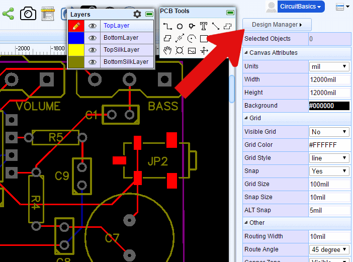
There is an option for that in PCB canvas attributes:
Before routing the PCB, the components need to be positioned in suitable places on the PCB. In the PCB Editor, it can sometimes be quite difficult to select components by clicking on the silkscreen outline or the pads. To select and move them more easily, please use drag mode (Hot Key D) or click the Move icon in the PCB Tools toolbar:
Schematic: You can place a single pin connector from EElib, and then update its package.
PCB: You can place a top/bottom layer pad , and then route it with track.
You can add a # characater in the pin name/netlabel last text. You can use symbols that you are familiar with. You do not have to add a line above the netlabel name.
Yes but for any but the simplest PCBs, please see:
https://easyeda.com/forum/topic/The_best_way_to_design_a_PCB_in_EasyEDA-ThR3pwqIC
You can refer to Text of PCB section.
You can refer to Image of PCB section.
You can refer to Import DXF File of Import section.
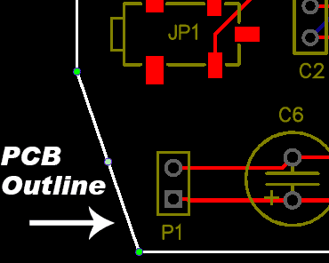
You can import a DXF file for the board outline. For a round board outline, you can use an arc to do that, you just need to change to the board outline layer, then draw 1 arc like in the image below (need to adjust a bit later), you can use lines and arcs to create complex board outlines.

Please use solid region https://docs.easyeda.com/en/PCB/PCB-Tools/index.html#Solid-Region
Or draw a track and right-click it, use the “Convert to NPTH” option.
https://docs.easyeda.com/en/PCB/PCB-Tools/index.html#Measure-Dimension
Click the layer options button, then tick the extra layers in the dialog that opens. https://docs.easyeda.com/en/PCB/Layers-Tool/index.html
It is possible to get boards with the copper exposed so that you can apply a layer of solder over those tracks to further increase their current carrying capacity. In this case, you need to add solder mask over a copper (copper area, track, solid region).
EasyEDA will add solder mask for pads automatically. Sometimes however, you may need to add an aperture in the solder mask to expose and area of copper.
First, add a top or bottom solder mask layer, as required.
Next, draw a region in the solder mask layer over a copper item as illustrated in the image below. This in effect draws an aperture in the solder mask so that the copper item inside the region, in this case the track, will be not be covered by the green film of solder mask.
A common mistake is to just draw a solder mask, without a copper area, like the track pointed to by the yellow arrow. That is incorrect and does not produce the desired result.
Or you can click the track, and then click the Expose Copper button at the right-hand panel.
PCB's dimension/size depends on the board outline, you can create your board outline, please refer to Board Outline of the PCB section.
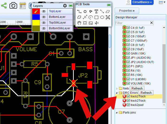
Please refer to Design Manager of PCB section.
You can use Unroute All and Global Delete under the Edit menu.
There are two ways to do this.
Bottom layer in the right hand panel.

When you create a SechamticLib, you can set the package for it at the right-hand panel.
When you at the schematic, you should select the component and click the package input box at the right-hand panel. and change it at Footprint Manager
When you want to change the schameticLib's package which was you had created, at “Libraries”, select the schameticLib, and click Edit button, click the package input at the right-hand panel, the footprint manager will show up, you can search or select the package and then update it, and then save the SchematicLib.
Please refer at PCB: Panelize
Please refer at Forum: What does Warning copper area do not allow self intersection

and Document > EasyEDA Source > Download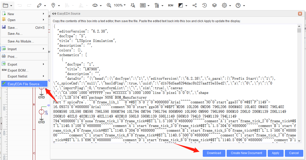
[email protected] or ask via our Support Forum; we will respond ASAP.Manually creating backup schematics into the same project. When a project is converted to PCB, EasyEDA will merge all of the schematics under the same project into a single PCB. If there are multiple copies of the same schematic in a project then this will create errors such as duplicate part prefixes. Especially if you are new to EasyEDA, just keep one copy of each unique schematic in any one project.
Saving schematic and PCB into different projects. Unless you are absolutely sure that you will not need to update (Synchronise) your PCB from changes made to your schematic then please keep the schematics and PCB under the same project.
Bad packages. Schematic symbols must have the appropriate footprints assigned to them, these footprints must exist in the library, and for any footprint that you have not created yourself, you must have clicked on the Favorite option in the component search window to add it to your Favorite Parts list in the left hand Navigation panel.
Using the polyline from the Drawing Tools Palette to connect symbol pins. To connect components together, you must use Wires from the Wiring Tools Palette.
EasyEDA's main target is schematic and PCB, not simulation. EasyEDA only support simple schematics simulation.
You can use the name attribute. Just set the name or double click the value text.

Voltage probe

EasyEDA only has very few simulation models, EasyEDA is powered by http://ngspice.sourceforge.net/ please check Ngspice to know what can be simulated.
Yes and no.
It uses X and Y coordinates where the horizontal X coordinate is positive to the right of the origin and negative to the left but the vertical Y coordinate is positive below the origin and negative above it.
Actually, we think our coordinate system is not very good but it is hard to change.

Version Rule
EasyEDA version number is ReleaseYearCount.ReleaseMonth.ReleaseCountOfThisMonth. For example, v4.9.3 is the fourth year release of EasyEDA, and at the ninth month of this year, EasyEDA had released 3 times.
Version Upgrade
If you use EasyEDA online, it can seamlessly upgrade by itself. However,EasyEDA uses an App Cache technique to allow you to use EasyEDA offline (W3C HTML5 Offline Web Applications) which may delay the automatic upgrading process. Therefore, if you want to upgrade to the latest version immediately, you can follow the two simple steps below.
Check the About… dialog;
If the Built Date is older than 2017/06/01:
Close your browser open EasyEDA again.
If the Built Date is still showing older than 2017/06/01:
Close your browser and open EasyEDA again.
If the Built Date is at or newer than 2017/06/01, you don't need to do anything.
Note: 2017/06/01 is just an example.
If those two steps don't work, you may need to clear your browser's cache:
1.Mozilla Firefox
Close the editor, Go to “Preferences… > Privacy & Security > History > clear your recent history” or use Ctrl+shift+Delete,
Click on “Clear now”,
Reload easyeda again.
2.Chrome
Close the editor, Open the following URL: chrome://appcache-internals/
Look for easyeda.com and click “Remove”
Reload easyeda again.
Or you can use Ctrl+shift+Delete to delete Chrome caches.
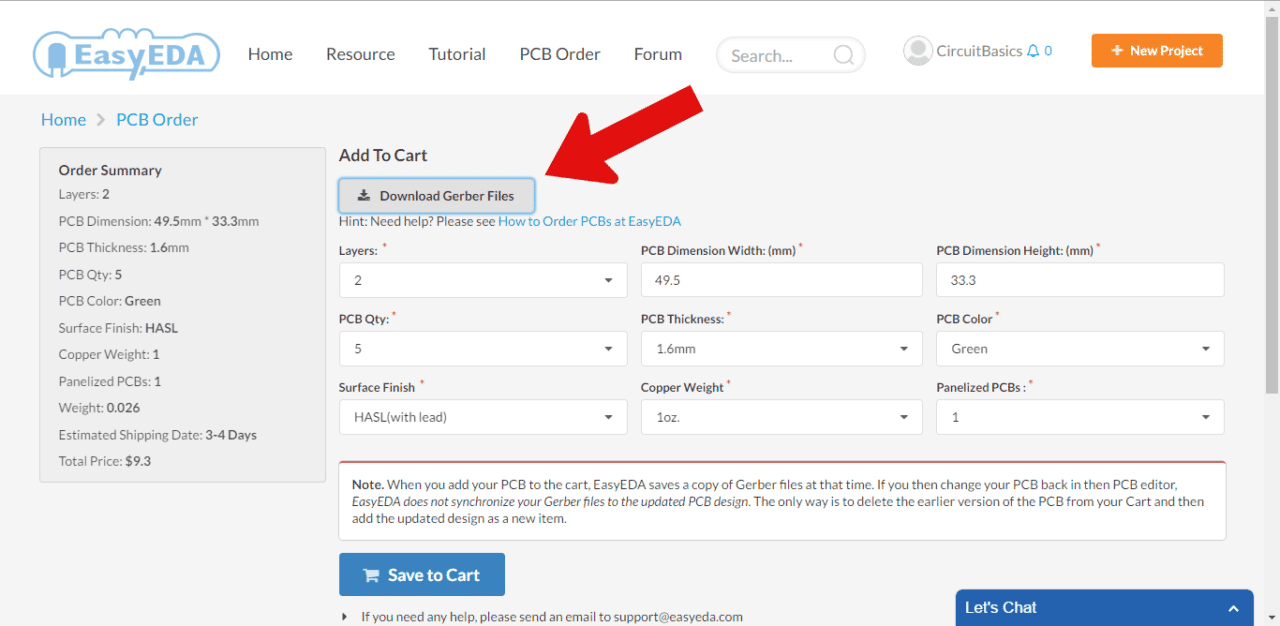
Before ordering, please check this Gerber first:
https://docs.easyeda.com/en/PCB/Gerber-Generate/index.html#Gerber-View
Visit and login at https://jlcpcb.com/quote
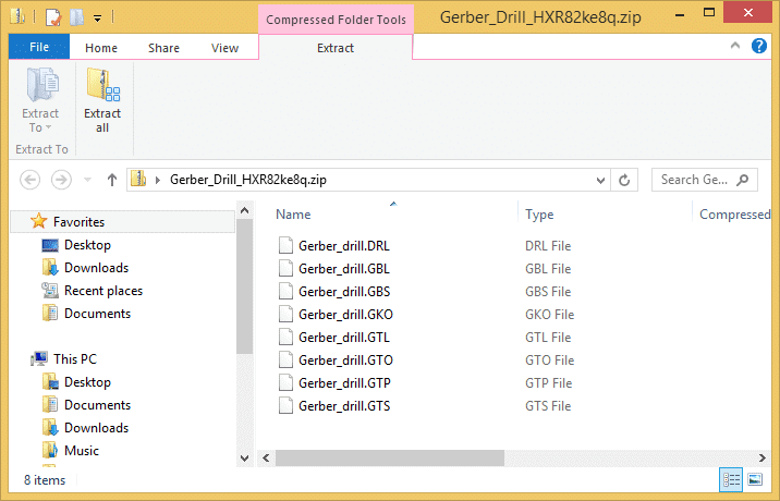
Add this Gerber file(compressed file) on the page and type the order options
Save to Cart, and then submit the payment
If you want to combine the components order with the PCB order at https://lcsc.com , please refer:
https://support.lcsc.com/article/24-do-you-offer-combine-shipment-with-pcbs
By following - and constantly checking against - a set of procedures, it is possible to avoid just about all of the common mistakes and omissions that can significantly delay or even stop a schematic being successfully converted to a PCB and then that PCB being successfully updated from the schematic as a design progresses.
It can also significantly reduce the likelihood of a PCB being made that subsequently is found to not work correctly due to mistakes made during the creation of the original schematic (Schematic Capture).
After spending hours on Schematic Capture, it is very frustrating to be presented with error messages about prefix conflicts, missing or invalid packages when first attempting to pass a schematic through to the PCB Editor by clicking on the Convert Project to PCB… button or, after making changes to a schematic, similar error messages or having components that disappear from the PCB when attempting to update an existing PCB using the Update PCB… button in the Schematic Editor or the Import Changes… button in the PCB Editor.
These issues can be avoided by running through a series of checks for the first time each new Part (i.e. the first instance) is placed into the schematic.
There are several other issues that arise from mistakes in and omissions from the schematic that people encounter only after they are part way through a PCB design or - worse still - only when they receive their PCBs in the post.
Almost all of these other issues can be avoided by running through a further series of checks (i) during Schematic Capture, (ii) once Schematic Capture is complete but before first attempting to convert the schematic into a PCB and (iii) when updating the PCB as work progresses.
This document pulls together all the essential procedures to follow and things to check in the schematic before clicking on the Convert Project to PCB…, Update PCB… or Import Changes… buttons.
Before using the document it is important that the following points are clearly understood:
A Part is any element of the circuit that is to be mounted on the PCB plus any element which is ultimately intended to be mounted on or form an integral part of the PCB such as heat sinks, PCB mounting holes, mounting holes for PCB mounted potentiometers and switches (for example where a PCB is used as a front panel or as a self-contained test jig), test points, wire links or jumpers, fuse holders and even image based elements such as high voltage warnings and logos.
Note that fuses that are fitted into PCB mounted fuse holders are best dealt with in a schematic by showing the fuse using a fuse symbol in the schematic but assigning to that fuse symbol the BoM information - including the package - that is for the required fuse holder. The required fuse ratings, type and supplier information can then be included in the BoM using Add new parameter function.
Other socketed devices can be treated in the same way.
Any Part must have a Schematic Symbol to represent it in the schematic (a.k.a. Schematic Lib) and that Schematic Symbol must have a PCB Package (a.k.a. PCB Lib) assigned to it either when the symbol is created or after placing the first instance of it into the schematic.
The associated PCB Package must exist in the library.
It is possible that a component may comprise more than one device in a package, for example logic gates. Some symbols represent both devices in a single symbol but quite often a separate symbol is used to represent each of the devices. This may mean that some of the pin numbers and/or names on the symbols representing each of the two devices may be different although both may have the same power and ground pin numbers and/or names.
High pin count devices such as processors and FPGAs may be split into several symbols representing different sections or ports. It is important to ensure that pin numbers and names are unique across all the symbols.
It is possible that a component may be available in different packages. For example the LM358-N dual operational amplifier is available in several different packages. The pin numbering and/or naming of the symbol may be different depending on which package the component is supplied in.
It is easy in EasyEDA to change the pin numbering and/or naming for a Schematic Symbol (using the I Hotkey) or a PCB Package so it may be tempting to think of an LM358-N as the same part in a different package and just put down a symbol, edit the package assigned to it and then hack the pin numbers and names about until they match the PCB package.
However, an LM358-N in a SOIC-8 package has a different pinout, a different part number and has to be physically ordered as a different part from an LM358-N in a DSBGA-8 package.
When thought of like this it should be clear that there should be one Schematic Symbol (or pair if each device has a separate symbol) and a matching PCB Package for an LM358-N in a SOIC-8 package and another Schematic Symbol (or pair if each device has a separate symbol) and a matching PCB Package for an LM358-N in a DSBGA-8 package.
It is important to understand that any Part that is supposed to form part of or be mounted on the PCB must have a corresponding Schematic Symbol in the schematic.
If it does then as soon as the PCB is created, the PCB Package for that Part , even such a seemingly abstract item as a mounting hole, warning sign or a logo, will be pulled into the PCB layout without having to be added to the PCB later by hand.
If it does not then not only will the PCB package for that Part not be pulled into the PCB layout as it is created but when it is added to the PCB later by hand and the PCB is then updated to bring in changes made to the original schematic, that PCB package will be deleted.
Such elements can be added to the schematic later and then imported into the PCB but if they do not exist in the schematic at the time the PCB is updated from that schematic then they will always be deleted and will therefore have to be added back to the PCB by hand.
Any Schematic Symbol or PCB Package chosen from the User Contributed category MUST be added to your local library by doing:
Libraries (or SHIFT+F) > Search for and select the part then > More > Add Favorite/Clone

Packages in the other library sections will be found automatically.
Note however that although Schematic Symbols and PCB packages created by a user within a Team will automatically appear in that user's My Parts library, once that user swaps to another Team, those parts will no longer appear in their My Parts library but will only be available via the Add Favorite option from the User Contributions library.
The schematic must help the reader understand signal and power flow in the circuit with inputs on the left, outputs on the right, positive supplies at the top, negative supplies at the bottom and netlabels used to clarify connections and reduce congestion.
Components may be grouped by function and boxes may be drawn around them.
Decoupling components may be drawn adjacent to the devices they are associated with or symbols with dedicated sub-parts for power pins can be used to reduce congestion;
Naming nets instead of relying on the EasyEDA auto-generated alphanumeric names makes signal tracing and debugging the final PCB much easier but care must be taken to ensure that names are correct and that there are no unintended duplicate names or accidental increments in numbered nets;
https://easyeda.com/forum/topic/How_to_resolve_quotPrefix_Conflictquoterror-gpbca8642
Remember to check across all sheets of a multi-sheet schematic;
Check that the schematic is drawn correctly.
In particular, check that no nets have been accidentally cross connected, that wires have join dots where they are intended to be joined, that they are properly connected to component pins and that nets joined by netlabels are correctly named and that there are no unintended duplicate net names.
Verify that junctions of 4 or more wires are drawn to show staggered junctions to avoid confusion with wires that cross but are not joined at the crossing point.
Check that all parts and nets have been placed with the Canvas Attribute Snap = Yes:
and that no parts have been placed off grid so that although they may appear to be connected on close inspection it can be seen that they are not:
Check that pins have been terminated (pulled up, down, left open etc.) as specified in manufacturers' datasheets.
Check that all unconnected pins have No Connect symbols attached directly to them. Unconnected pins without No Connect symbols attached directly to them will show up as alphanumeric net names in the Design Manager but will not highlight when clicked on in the Design Manager.
No Connect symbols must be attached directly to component pins. There should be no wire between the No Connect symbol and the pin.
Note that the No Connect symbol changed in V4.8.5 of EasyEDA from a red cross to a green one to make the highlighted state of a selected symbol clear;
Check that the device ratings are suitable for the circuit in which they are to be used. For example, capacitor, diode, transistor, connector and switch voltage ratings, transistor, resistor and zener diode power dissipations, inductor, diode (including LED), transistor, connector and switch current ratings.
Although these parameters should have been checked at the time of specifying the components as an essential part of the circuit design stage prior to or during Schematic Capture, there is plenty of scope for them to have gone astray during the part selection, placement and editing steps of Schematic Capture.
An undetected mistake now can result in the wrong size part being chosen. For example a larger diameter or even a taller electrolytic capacitor may be needed. Whilst this is easy to correct in the PCB design stage, at best this may waste time in having to redesign part of the PCB. At worst the mistake may not be discovered before the PCB design is completed and sent for manufacturing.
Consider adding diode or MOSFET reverse supply protection especially for battery powered circuits.
An example of MOSFET reverse protection is described in:
https://easyeda.com/example/Uberclamp_Schematic_PCB_and_BoM-r4YgysK2k
Pay special attention to this in operational amplifier or comparator devices that exhibit output phase reversal under some input conditions. For more information about this see:
http://www.analog.com/media/en/training-seminars/tutorials/MT-036.pdf
For example, the TL081 exhibits this behaviour but it is not documented in more recent versions of the datasheet. See Applications Hints on page 5 of this earlier version:
http://www.physics.ucc.ie/fpetersweb/FrankWeb/courses/PY2108/spec%20sheets/TL081%20OpAmp.pdf
Consider adding diode or MOSFET reverse supply protection especially for battery powered circuits.
An example of MOSFET reverse protection is described in:
https://easyeda.com/example/Uberclamp_Schematic_PCB_and_BoM-r4YgysK2k
For background on this please see:
https://easyeda.com/andyfierman/LEDs_must_have_series_resistors-OoGYgCK2k
Check that signal connectors have sufficient ground pins to maintain signal integrity by minimising signal return path impedances (i.e. ground loop area). This is especially important in designs with high speed signals through the connectors but can also be important for lower speed signalling with long wire interconnects and/or fast edge speeds.
Check that power connectors have sufficient ground and power pins pins to maintain power integrity by minimising power and ground return path impedances.
Verify that device power supply decoupling complies with manufacturers' recommendations.
Where possible, check datasheets, applications notes and schematics and PCBs for Reference Designs or Evaluation Boards.
For some background on the importance of adequate decoupling please see:
Remember to include Schematic Symbols and an associated PCB Packages for things like heat sinks, PCB mounting holes, mounting holes for PCB mounted potentiometers and switches (for example where a PCB is used as a front panel or as a self-contained test jig), test points, wire links or jumpers, fuse holders and even image based elements such as high voltage warnings and logos;
Look in:
Libraries (or SHIFT+F) > SCH/PCB Lib > Personal > Favorite
 for every Part are correct, unique and match those of the PCB package's pad numbers associated with that particular part;
Verify that the pin order (pin mapping) of the PCB Package associated with every part is correct.
This task is simplified using the EasyEDA Footprint Manager:
https://docs.easyeda.com/en/Schematic/Footprint-Manager/index.html

Remember that in EasyEDA, the PCB Footprint is viewed looking down onto the component side of the board. This view is assumed to be with all components mounted on the Top Layer. Packages can subsequently be placed on the top or bottom layers as required.
For more information about this please see:
https://easyeda.com/forum/topic/How_to_add_extra_information_to_the_Bill_of_Materials_BOM-Hp9rJCUcu
Including text (or even diagrammatic information in the schematic about component positioning and orientation, clearances around heatsinks for airflow or copper areas for heat sinking, current and voltage ratings of traces, trace length matching, controlled impedance transmission lines and differential pairing can all help in the following stages of PCB design.
Nets that are carrying high currents may be drawn using thicker wires (Stroke width).
Nets can be drawn converging at star points to help illustrate where this type of PCB layout is required on the PCB:

Kelvin connections to current sense resistors can be drawn in a similar way:

Nets can be colour coded but beware using red because it can be very hard to see when such nets are highlighted.
Whilst it is easy to change parts in the PCB design stage, at best this may waste time in having to redesign part of the PCB. At worst the unavailability of a part may not be discovered before the PCB design is completed and sent for manufacturing.
In this PCB layout tutorial I hope to tell you how to create a good PCB layout very easily and clearly. I'd like to take EasyEDA PCB design editor as an example because it's free, easy-to-use and without any installation but it brings you fast PCB design and easier circuit design experience.
Step 1: Convert your schematic to a PCB First you could draw your schematic on EasyEDA editor as below image showed. I'm using this music controlled LED's schematic for this tutorial:

Once you're done with your schematic, you could click on “Convert project to PCB”

Step 2: Placing the components Now it's time to drag and drop the components to the spots where you want them to be. If you want your PCB to look as clean as possible I suggest placing all components with the same function next to each other, like resistors for example. Also make sure to leave some extra space between components, especially capacitors since the size may vary. Apart from the fact that the size may vary leaving some space will make the soldering a lot easier. Especially when you have to solder SMD components.
Step 3: Drawing a custom outline First, select the “BoardOutline” layer in the layers menu:

Click on the current outline (the pink square in your editor) and press delete to get rid of it.
Now you can use the PCB tools to draw a new outline:

Once you're done with your outline you can switch back to either the top or bottom layer.
Step 4: Creating a copper area (GND) A very easy way to connect a lot of parts to a signal (mostly used GND) is to create a copper area. You can create a copper area by using the tool “Copper Area” in the Tools menu. Once you're done drawing just outside of the outline your PCB should look something like this:

Now click on the dotted line you just drew and check whether these settings are correct. Once they are correct you can click “Rebuild CopperArea” and your PCB will be filled with copper only connecting to GND.

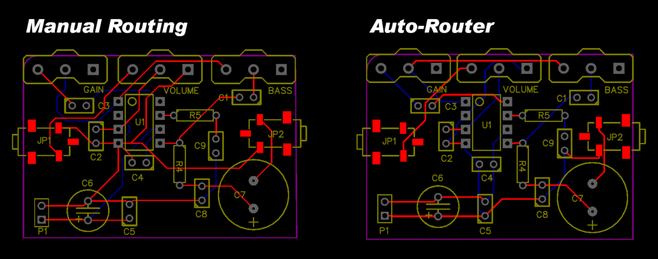
Step 5: Routing There are 2 different ways to perform this step. The easiest is to use the “Auto Router” function. If you're creating a PCB where the current is low you can use this method, but if you need different track sizes you're better off routing the PCB yourself. The Auto Router function can be found here:

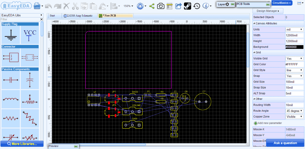
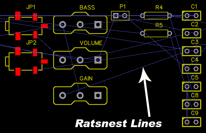
You should see blue lines all over the PCB. These indicate which component's pin is connected to which pin.

Now use the “Track” tool in the tools menu and click on a pad. Once you move your mouse you should see the blue line moving as well. Make sure not to cross any other tracks or pads and start routing all tracks to the correct pads.
You can switch to the opposite layer (top/bottom) if you have to cross lines.
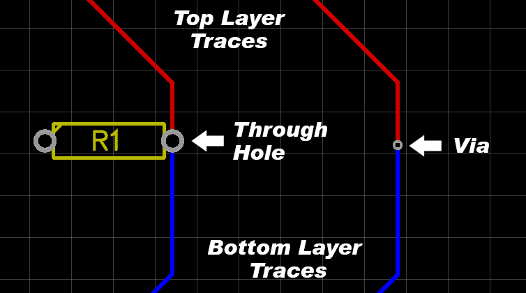
If you have to switch to another layer for a SMD component you have to use a “via” which can also be found in the tools menu. A via is basically a copper connection between multiple layers.
This is an example of what your PCB could look like (With “Fill Style” None in the copper area properties):

Step 6: Adding holes If you want to mount your PCB onto something it might be useful to add some holes. Click on the “Hole” tool in the tools menu. Now you can set the size of the hole on the right. Make sure you're using the right units!! Once the size has been set you can click on the spots you want your holes to be. Don't place holes onto components or tracks. Resize your PCB outline if you need more space to add the holes.
Step 7: Adding Text and Images To add text click on the “Text” or “Image” tool in the tools menu. Place the text where you want it to be and change the text in the right properties menu. You can also change the desired layer in the menu.
Step 8: Finalizing the PCB You can take a look at the finished result by clicking on the “Photo View” button:

Once clicked you can find different options like top/bottom side, but also the color of the PCB.
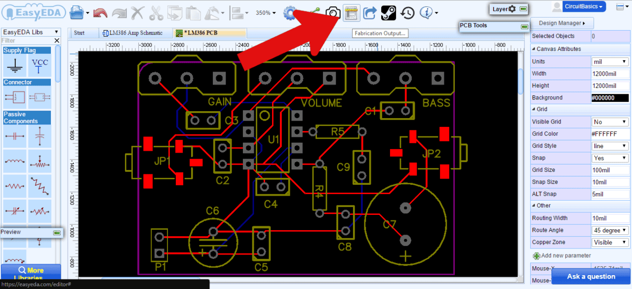
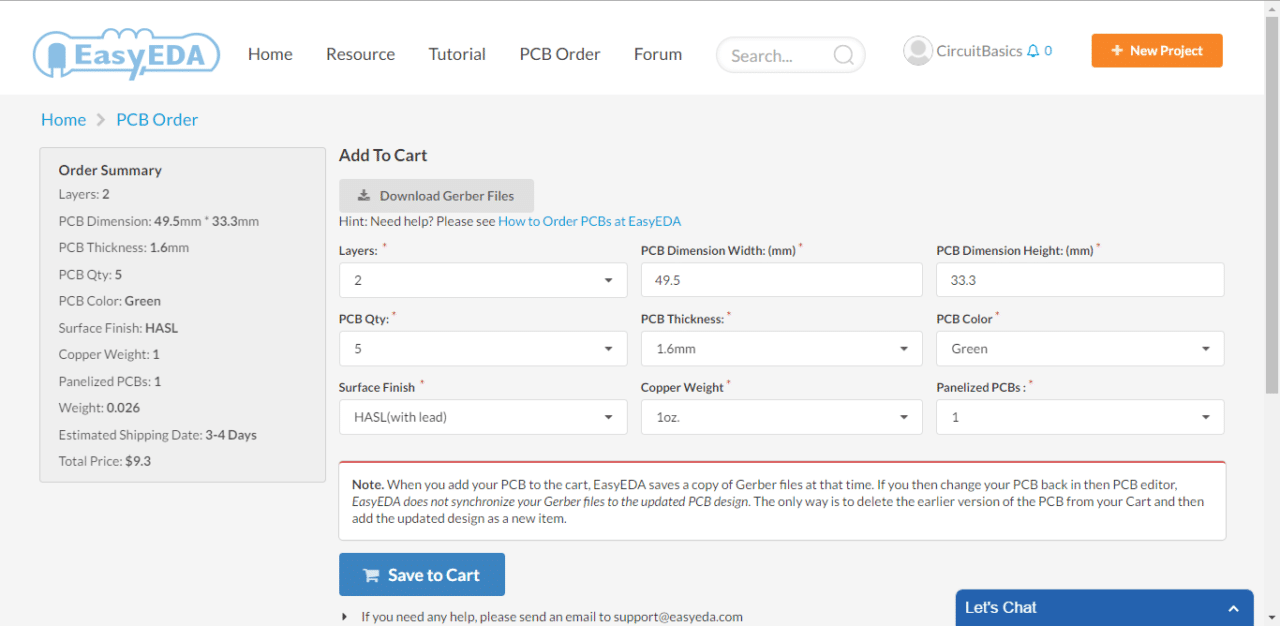
Once you're satisfied with the result you can click on “Fabrication Output” to buy the PCB's using the service EasyEDA is also providing.

I hope this PCB layout tutorial has helped you improve your PCB designing skills. If you are interested in creating your PCB and learning how to manage EasyEDA PCB design editor, you could check this video and more step by step tutorial.
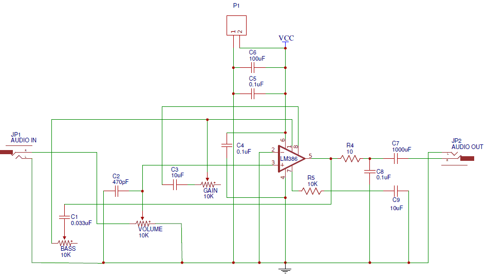
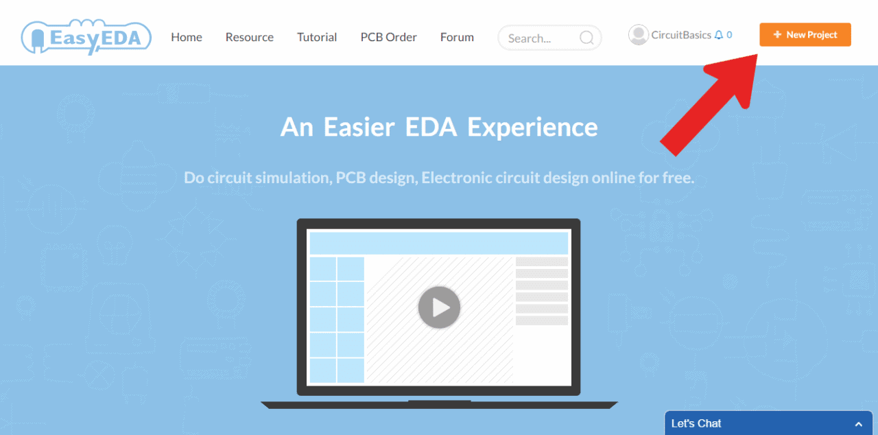
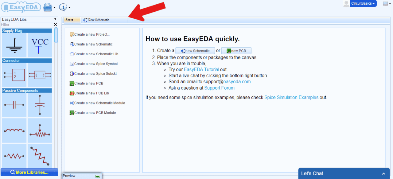
 It's best to place all of your schematic symbols on the canvas before drawing any wires. In EasyEDA, schematic symbols are located in “Libraries”. The default EasyEDA library has most of the common symbols, but there are also “User Generated Libraries” with lots of other symbols:

